(My main goal is to be informative and explain the path i have followed. It may have little complicated, But im open to your comments)
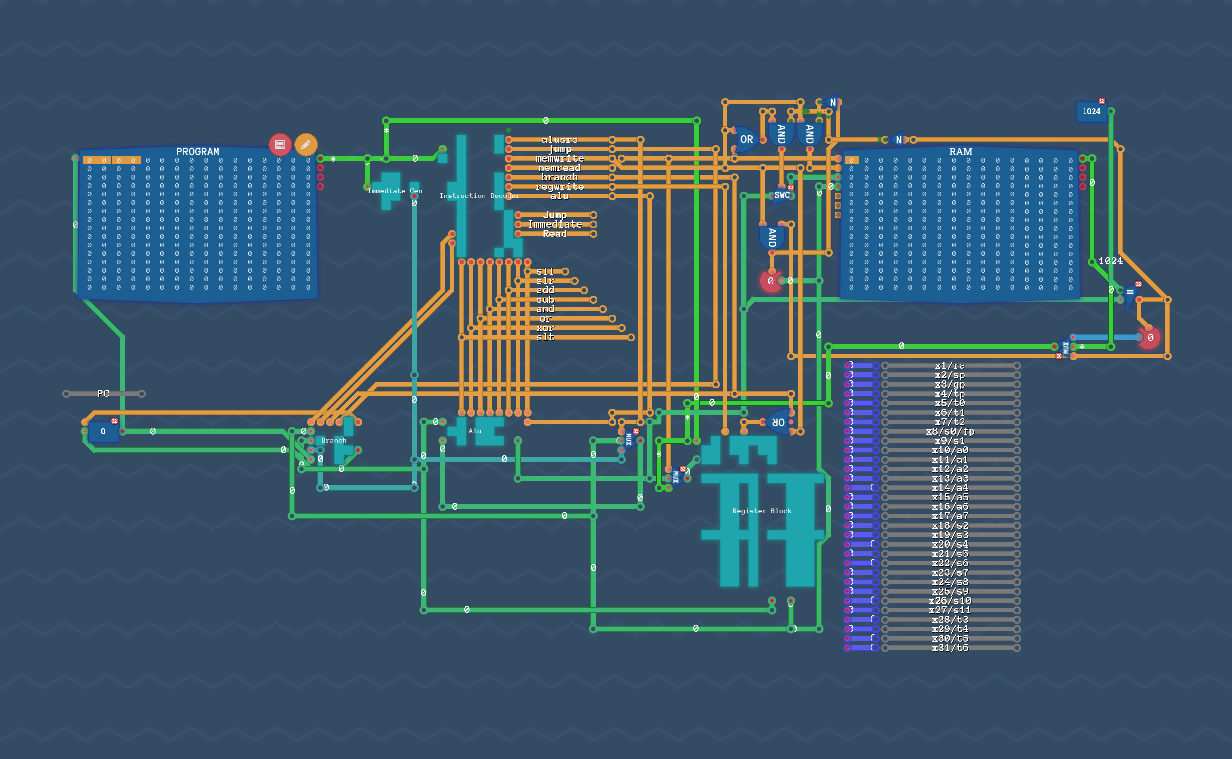
Firstly, I decided to build my own basic RISC-V because the processor that gave from the game (Built from scratch on the games route) not enough for me, and we can build anything in this game and i discovered processor types CISC,RISC after than i decided to build basic RISC-V.
Up until that day, i know these concepts:
- Instruction decoder
- Alu
- Branch
- Registers (Immediate, Read types)
but that day i need more realistic CPU design. Firstly i started from Instruction Types in RISC-V and their alignments.
R-type: register-register
I-type: short immediates and loads
S-type: stores
B-type: conditional branches, a variation of S-type
U-type: long immediates
J-type: unconditional jumps, a variation of U-type
My brain said "im out" i really not understand but im not CPU designer my target is just understand the concept how working.
so i choose only (I,R,J) (enough)
After than i made a Instruction Table

For Read instructions, I decode this alignment structure =

For Immediate instructions, I decode this alignment structure =

And i designed in game with Equal and Constant components (i know its like wire spaghetti)

And i was started to make Register block (This was the hardest part for me)

In Register Block, Firstly i decode the alignment. If the opcode is Immediate type, I move Return Address to Read Address 2 with MUX component.
In this decode part i learned how computer address it. Firstly i decode the part, now we have 8 bit value. And we shift left 1 value in 32 bit with that 8 bit value to get address. Normally we want 5 bit decoder with 32 output because 5 to the power of 2 equal to 32 and we have 32 register, with SHL component we do that easily without 5 bit decoder.
An example:
We need to reach 10. Register. We gave to opcode 10 = 00001010,
We gave 1 bit to SHL value section. And we gave our opcode to SHL shift by section. Result, 1 is shifted ten times and we got 0000 0000 0000 0010 0000 0000
and we would use 32 byte splitter, 32 byte splitter gives 8-8-8-8 output, and we use 4 8 bit splitter to get value.

So we have 32 output.
Anyway, We have 2 (1 bit input)

If the RegWrite flag is on, RA register's save section gonna on, And if we gave a value to Register Block, that will gonna saved to RA.

Load section is on everytime. Because we control read permission with switches
and register block outputs 2 value (arg1 and arg2).

I connected these outputs to ALU and i made Immediate Gen block. If the opcode says its a Immediate value, Alu takes IM value instead arg 2

Alu (Arithmetic logic unit)

SLT: Signed Less Than
XOR: or. (but not both)
SLL: Shift Left Logical
SRL: Shift Right Logical
For jump types, Thats a branch block controls branch types and jump, and changes the Program Counter(PC).


and its check BEQ,BNE,JUMP.
BEQ: Branch if Equal
BNE: Branch if Not Equal
and these branches uses jump with offset i mean if we give 5 value, and if the branch triggerred, PC jumps = (Current PC val + Offset). Like this
BEQ x10,x11,2
ADD x12,x10,x11
XOR x12,x10,x11 (BEQ JUMPS HERE)
but JUMP directly jumps to the our value
XOR x12,x10,x11 (JUMPS HERE)

JUMP 0

ADD x12,x10,x11

ADD x12,x10,x11
And the last thing is ram. I connected Alu's result to ram's address section.


LW: Load Word
SW: Save Word
We use these instructions to save and load values in ram.
These instructions work like add, because they are working like that. But we using for addressing.
LW SrcRegister, BasePointer(gets from register), Offset (gets from IM)When i writing my own assembly, i noticed i really understood Base pointers, Stack Pointers and more because in the past when i reverse engineered any file, i didn't understand the offset, addressing and more but with these practices, i really understand.
I said stack but if we talk more detailed, stack works like this schema
if any function is going to call
we push our args, return address to stack
firstly calculates how many values we need to push into stack
an example we have 5
ReturnAddress, Number 1, Number 2
Now this functions offset is 3
we push like that before we call function in the function (because we dont wanna lose the values)
Before push
- BP: 255 (Max of ram)
- RA: 0
and the stack is empty.
subi bp,bp, 3 // bp = bp - 3
sw x10(Number 2), bp, 0 (offset)
sw x11(Number 2), bp, 1 (offset)
sw x11(Number 2), bp, 1 (offset)

sw x2(Return Address), bp, 2 (offset)
push works like that.
After push
- BP: 253
- RA: 1 (its temp, so i gave random number)
and the stack looks like this (stack is a group name, its keeping on the ram but at the end)
address view
- 251: 0
- 252: 0
- 253: x10
- 254: x11
- 255: RA
function a(Number 1, Number2)
	//When the b function ends, we get our last values in stack
	a = function b(Number2, Number 1)
	//Return Jumps here and we got last values that we use.

function b(Number1, Number 2)
	return,
	(In there, Our program POPs last values into registers.)

##In Assembly
lw x10(Number 1), bp, 0 (offset)
lw x11(Number 2), bp, 1 (offset)
lw x2(RA, Return Address), bp, 2 (offset)
//We're done, restore to original state
addi bp,bp, 3  // bp = bp + 3
// return jumps to RA
jump RA 
And i made a control mechanism to check input and output components but nevermind,
If the LW called, MemRead flag gonna open, Its open Rams Load input and Changes MUX to Ram Out. That means Ram Out value going to directly Register block (Read).
If the SW called, MemWrite flag gonna open, Its open Rams Save input and Changes MUX to original path. And the Reg 2 gives value, Ram's save flag is opened, Address got from Alu, and the value is saved into ram!
Finally i really understand assembly and how processor work with this project. I did it in 4-5 days (but i had worked on it for 15-20 hours)